In today’s rapidly evolving technological landscape, the demand for electronic products has surged, leading to increased concerns about electronic waste and environmental sustainability. As industries seek more eco-friendly manufacturing methods, printed electronics have emerged as a promising solution. Among the various technologies driving this shift, High Precision Capillary Printing (HPCaP) is playing a crucial role. This innovative technology is not only advancing sustainable manufacturing but also setting new benchmarks for precision and efficiency in the production of electronic components.
The Need for Sustainable Manufacturing in Electronics
The proliferation of electronic devices in our daily lives has brought about significant environmental challenges. From smartphones to electric vehicles, the demand for electronics is at an all-time rise, and so is the production of electronic waste. Traditional manufacturing processes, particularly in the electronics industry, are resource-intensive and often involve hazardous materials, leading to a considerable environmental footprint.
To address these challenges, the industry is turning to sustainable manufacturing practices that minimize waste, reduce energy consumption, and utilize eco-friendly materials. Printed electronics, which involve the creation of electronic components through additive manufacturing processes, are at the forefront of this shift. Unlike traditional subtractive methods, where materials are removed to create components, additive manufacturing builds components layer by layer, using only the necessary amount of material. This approach significantly reduces waste and energy usage.
High Precision Capillary Printing: A Game-Changer in Printed Electronics
High Precision Capillary Printing (HPCaP) is a cutting-edge technology that exemplifies the potential of printed electronics to revolutionize manufacturing. Developed by Hummink, a leading innovator in the field, HPCaP offers a precise and efficient method for printing electronic components on a variety of substrates.
The technology relies exclusively on capillary forces to drive the printing process, making it highly efficient and eco-friendly. Unlike traditional printing methods HPCaP ensures complete utilization of materials within the printing pipette, resulting in a zero-waste process. This precision is particularly beneficial in industries such as semiconductor manufacturing, where even the smallest material waste can lead to significant cost increases.
How HPCaP Works: Precision and Efficiency
HPCaP technology draws inspiration from Atomic Force Microscopy (AFM) and uses a macro-resonator as its primary sensing mechanism. This resonator oscillates at a frequency of about 1 kHz and is attached to a mechanical bridge. By controlling the resonance phase, amplitude, and frequency, HPCaP can achieve different printing features, such as varying the thickness and line width of the printed material.
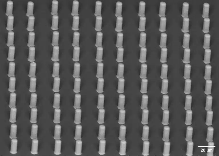
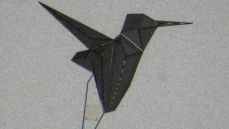
A glass pipette attached to the macro-resonator is used to dispense the ink. The real-time detection of the interaction between the substrate and the pipette prevents any damage to either component while maintaining a high-quality dispensing mechanism. This level of control allows HPCaP to print micron-scale lines with remarkable accuracy, as demonstrated by the absence of splashes or satellite drops in the printed lines.
One of the key advantages of HPCaP is its ability to use small volumes of ink to produce extensive samples. For instance, a single pipette filled with just tens of microliters of ink can print distances of up to hundreds of kilometers, depending on the dispensing diameter. This efficiency not only reduces material usage but also lowers costs, making HPCaP an attractive option for sustainable manufacturing.

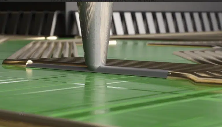
Schematic representation of the macro-resonator (right) where the glass pipette is attached and a close-up on the glass pipette in contact with a substrate.
Complementing Traditional Photolithography
Photolithography, a widely used technique in the semiconductor industry, is known for its high-resolution patterning capabilities. However, it involves numerous steps and consumes a significant amount of resources. HPCaP, while not a direct substitute for photolithography, serves as a complementary solution that can reduce the number of steps involved and offer comparable resolutions up to 100 nm.
In a comprehensive comparison, HPCaP outperforms photolithography in several key areas. For instance, it reduces the number of processing steps to only one and cuts down the processing time from for example 16 hours to just 0.5 hours. Moreover, HPCaP is more cost-effective, requires less space, and generates virtually no waste. These attributes position HPCaP as a valuable tool for manufacturers looking to enhance sustainability without compromising on precision or quality.
HPCaP in Action: Real-World Applications
The potential of HPCaP extends beyond manufacturing to include repair and remanufacturing, crucial aspects of promoting sustainability. By enabling the precise repair of electronic devices, semiconductors, and automotive components, HPCaP helps extend the lifespan of these products, reducing the need for new manufacturing and thereby minimizing environmental impact.
For example, in the display industry, the repair of thin-film transistors (TFT) and color converters at the micron scale is a growing challenge. Traditional repair methods often fall short of the required precision, but HPCaP excels in this area, as evidenced by its successful application in repairing TFT lines. Similarly, in the semiconductor industry, where manufacturing is transitioning from wafers to panels, the ability to repair metallization defects at the micron scale is becoming increasingly important. HPCaP meets these requirements, offering a high-resolution, zero-waste solution that improves repair yields.
The automotive industry, too, is benefiting from HPCaP’s precision. As vehicles become more technologically advanced, the demand for repairing and remanufacturing components at micron and sub-micron resolutions is rising. HPCaP’s ability to deliver this level of precision makes it an ideal solution for the automotive sector, contributing to the sustainability of the industry by reducing the need for new components and lowering overall emissions associated with manufacturing.

The Future of Sustainable Manufacturing with HPCaP
As the electronics industry continues to grow, the need for sustainable manufacturing solutions will only become more pressing. HPCaP technology, with its unique combination of precision, efficiency, and eco-friendliness, is well-positioned to lead the charge towards a more sustainable future. By minimizing material usage, reducing waste, and enabling the repair and remanufacturing of electronic components, HPCaP is not only advancing the field of printed electronics but also setting new standards for sustainability in manufacturing.
In conclusion, HPCaP represents a significant step forward in the pursuit of sustainable manufacturing. As industries around the world continue to grapple with the challenges of electronic waste and resource scarcity, technologies like HPCaP will be essential in creating a more resilient, efficient, and environmentally friendly future. With its proven track record and ongoing innovations, HPCaP is set to be a key player in the future of electronic manufacturing.


