Applications

Opening up to a wider range of manufacturing perspectives.

DISPLAY

SENSORS

PHOTONICS

LUXURY

PACKAGING

Boosting the semiconductor industry.

The semiconductor industry is the physical engine of growing digital applications: AI, Cloud, 5G, quantum, microLED, space.
But the industry is mostly held back by a manufacturing challenge: assembling ever more complex and miniaturized components.

Hummink has been collaborating with world-renowned industrial R&D partners to adress these challenges with concrete applications.

CEA Leti is a key European player in research, development and innovation in the semiconductor industry.
Together, we have been developing new solutions for advanced packaging and transparent conductive oxydes manufacturing.

CNES is the French National Center of Space Studies. It guides innovations for the aerospace and defense industries.
We have been collaborating on micro-electronics applications (sensors, interconnects, etc.)

Itodys Lab from Université Paris Cité is a printed electronics specialist with deep industrial connections.
Collaborating on printed electronic topics (graphene transistors, bio-sensors, nano-catalysts), and acquirers of the 1st Nazca machine in 2022.

Unique Patentend Technology​

The future is driven by nano-electronic objects, designed with growing complexity
and continual miniaturization. But the thing is: no one can assemble them.

Our Use Cases

Illustrative scenarios that spotlight the practical application and
transformative potential of our technology.

Want to draw micronic or sub-micronic patterns?

Manufacture, repair, functionalize or decorate the micro-objects of tomorrow

Meet our trusted partners.

Hummink has been collaborating with world-renowed industrial R&D
partners to address these challenges with concrete applications.

FAQ Application

Which industries can benefit from HPCaP technology?

HPCaP supports a wide range of industries, including semiconductors, display repair, sensors, photonics, biotechnology, luxury goods, advanced packaging, and printed electronics. Its ability to print any material on virtually any substrate opens opportunities across numerous high-tech applications.

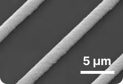
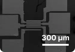
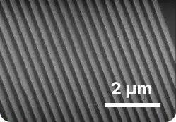
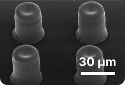
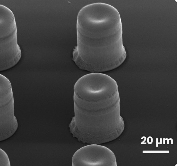
HPCaP enables highly localized repairs of TFT, OLED, and microLED displays by precisely depositing conductive, polymer, or color materials exactly where needed. Unlike conventional repair methods, it eliminates satellite drops and particle generation, making it ideal for next-generation high-resolution displays.