
Precision printing reinvented
at the micron scale
with the unique technology
High Precision Capillary Printing (HPCaP)


















The exclusive developer of HPCaP
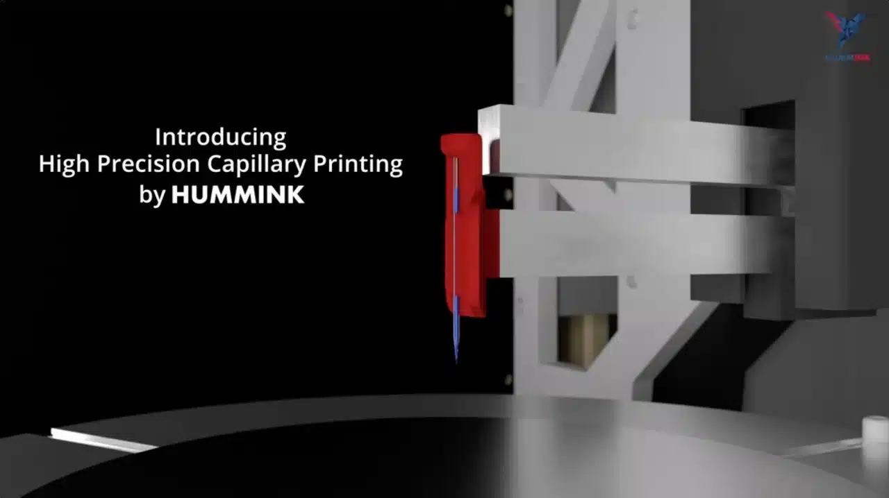
Hummink develops and supplies High Precision Capillary Printing (HPCaP), a patented technology enabling micron-scale material deposition for advanced electronics manufacturing. From R&D to industrial production, our integrated solution combines printing systems, intelligent software, and proprietary inks.
Already adopted by leading industrial and research organizations across Europe, Asia, and the US, HPCaP enables next-generation manufacturing and repair applications in displays, semiconductors, and advanced packaging.

Event
Meet us at SEMICON Europa 2026
A unique technology breaking down the 5 µm wall
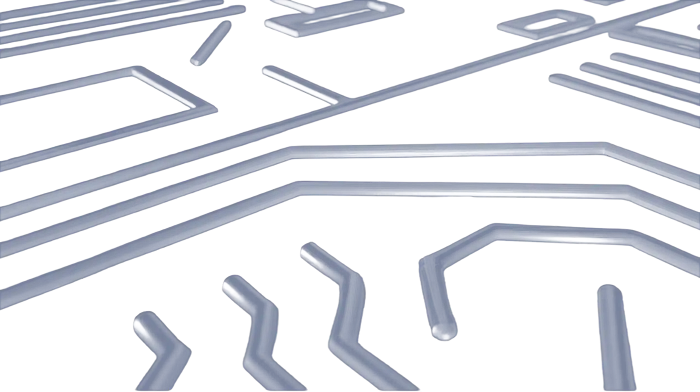
HPCaP prints below the resolution ceiling of conventional additive processes. No mask, no contact with the substrate, on flat or non-planar surfaces.
Resolution
Line widths from 80 down to 0.6 µm
Viscosity range
From 1 to 550,000 cP
Inks & substrate adaptability
Print across a wide range of inks and substrates
Discover our products
-

Printing Essentials
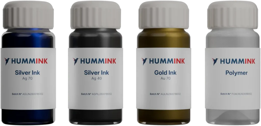
Inks and pipettes designed as one system. Centrifugink fills the pipette tip without bubbles and with minimal handling.
Proven in R&D, now in Production
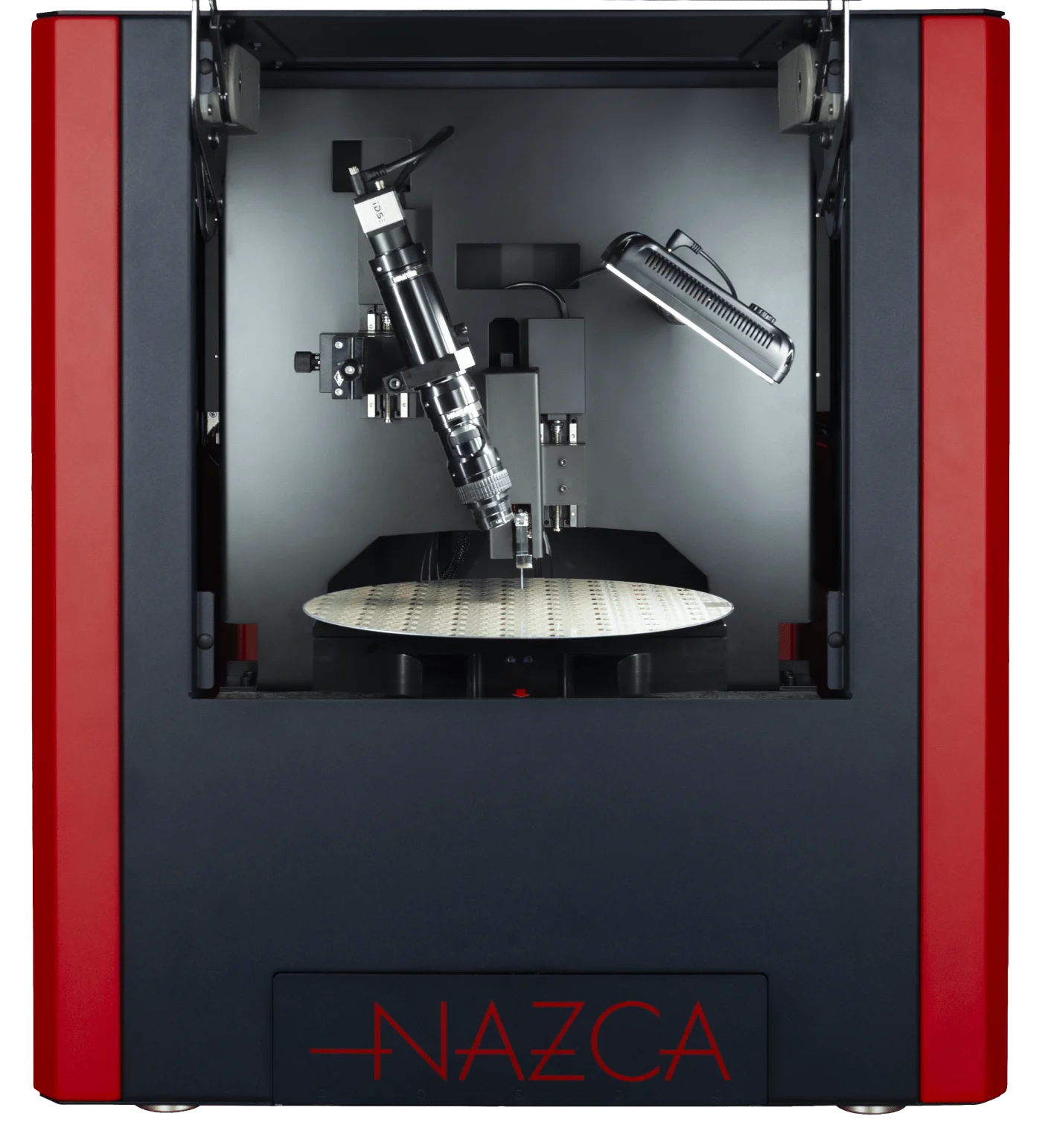
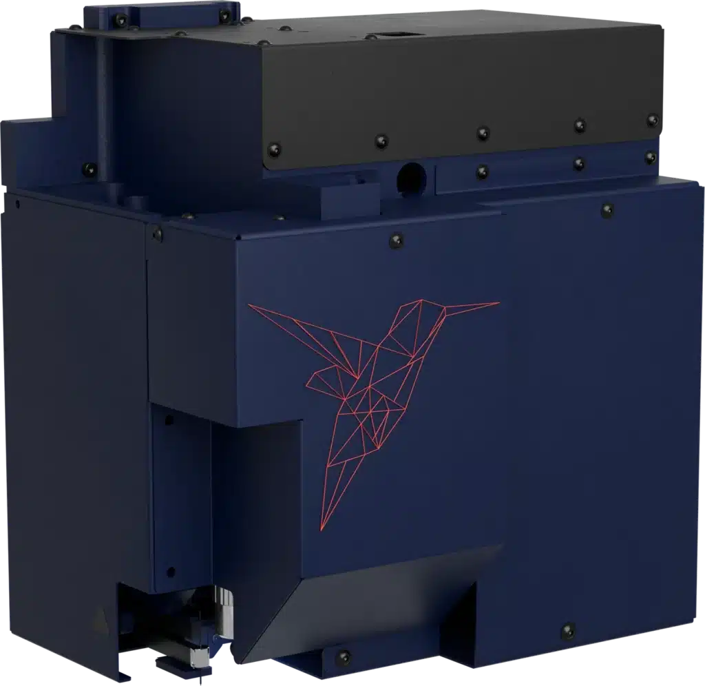
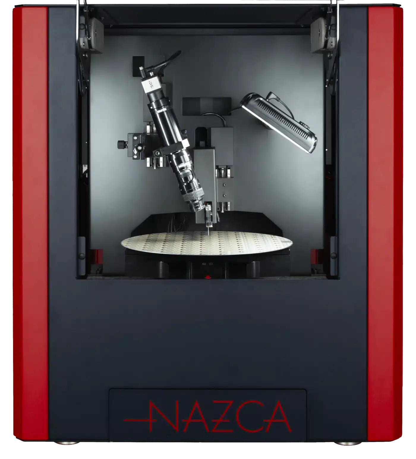
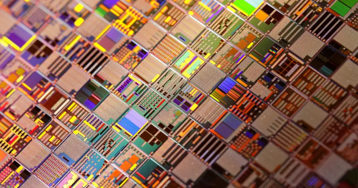
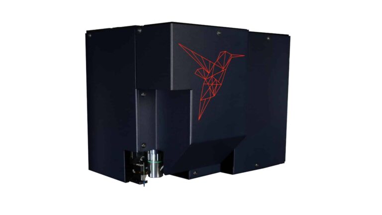
The BIRD module brings HPCaP to the production line, with in-line repair that corrects defects as they occur, enhances yield in AI chip manufacturing and opens a new path for advanced packaging. It builds on the same technology as the NAZCA tabletop tool, established in R&D labs around the world.
How HPCaP is transforming your industry
Interactive globe showing Hummink sales representatives and installed systems
Hummink around the world
Paris, Seoul, Tokyo, Shanghai, Taipei, New York
NAZCA
Paris, Bordeaux, Grenoble, Gardanne, Southampton, Luton, Boston, Durham, Gorgonzola, Seoul, Tokyo, Lecce, Kgs. Lyngby, Gardanne, Bienne, Taipei
Module
Seoul
They trust us

My team was amazed by how easy the Nazca tool is to use! Usually, a system with as many options as the Nazca has would take several printing sessions to enable someone to successfully print on their own; for Nazca, it only took one training. We are looking forward to exploring many uncharted paths to direct-printed electronics using this system!
Pr Aaron Franklin
Professor at Duke University


Hummink’s technology offers unique manufacturing possibilities by allowing various materials to be deposited at scales inaccessible with existing technologies in our laboratory as well as in the market. We have thus acquired their NAZCA equipment to carry out numerous research projects in micro-electronics, with a strong industrial dimension.
Pr Vincent Noël
Professor at Université Paris Cité

Our latest news

Frequently asked questions
What makes HPCaP different from other printing technologies?
Unlike droplet-based methods, HPCaP prints without satellite drops or splashes and adapts to uneven surfaces thanks to an integrated AFM with 5 nm Z-precision. It supports a wide range of inks and substrates while using very little ink.
What is the printing resolution?
The printing resolution of HPCaP ranges from 80 µm to 600 nm.
What force is applied to deposit ink with HPCaP technology?
HPCaP deposits ink by capillary force only, through a meniscus formed between the tip and the substrate.
Which industries use HPCaP?
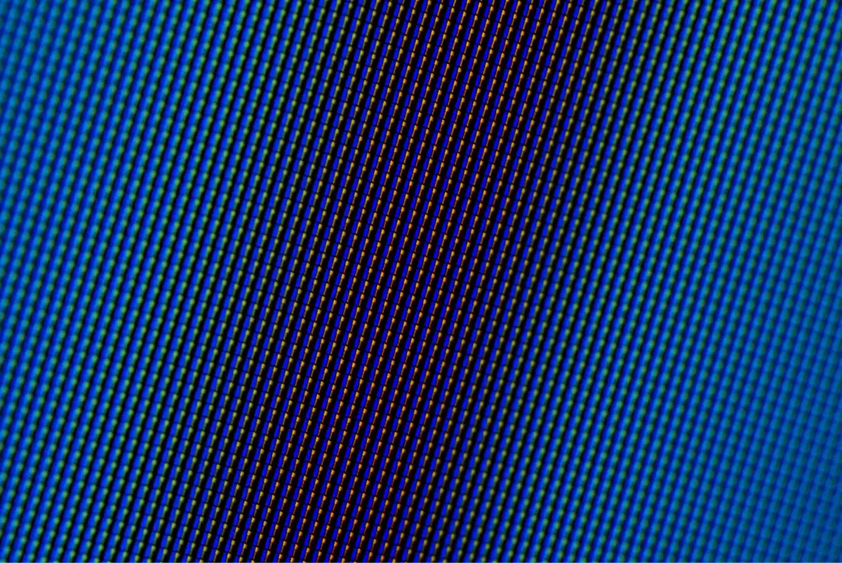
HPCaP addresses applications in semiconductors and advanced packaging, display and display repair, printed electronics and biosensors, MEMS, watchmaking, aerospace, defence, and advanced R&D.
Get started
Still unsure? We will help you find the right fit.
Talk to our team, we’ll help you match the right product to your volume and your lab.