Field of application
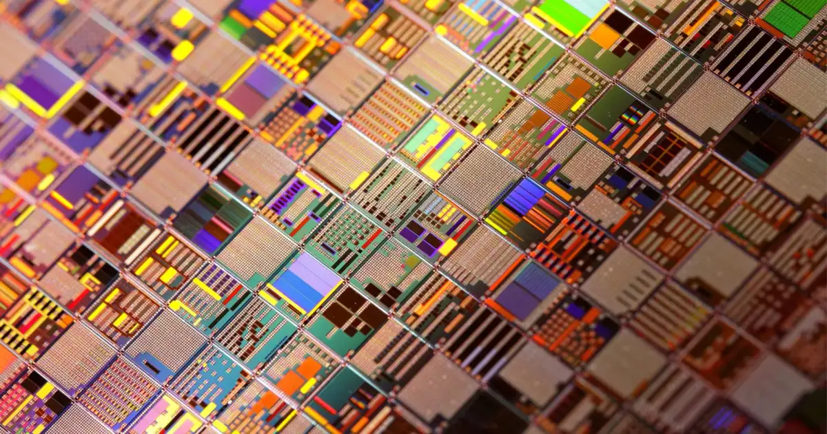
Semiconductors & Advanced Packaging
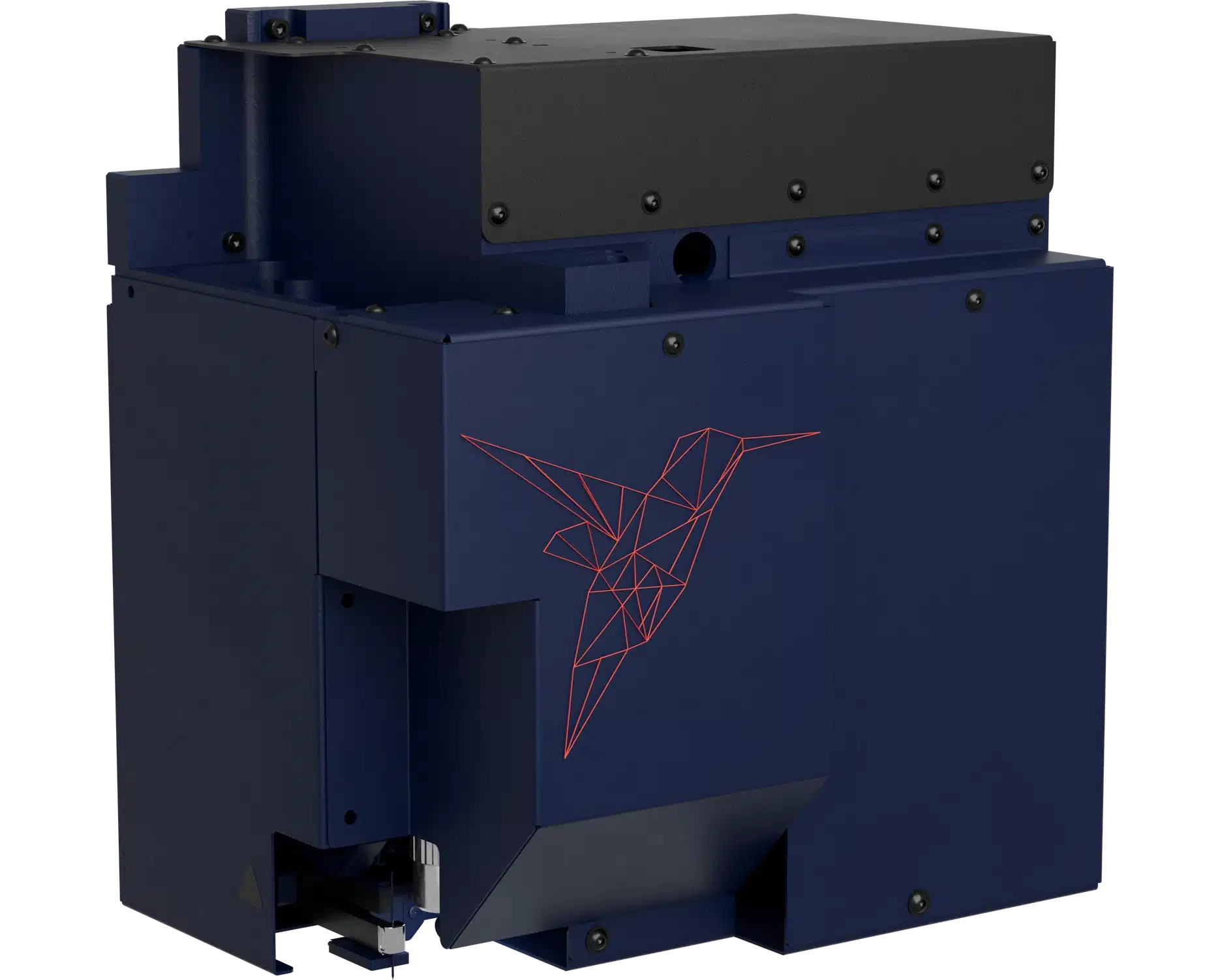
HPCaP enables targeted deposition of inks on display substrates, for production and defect repair
Market challenges
Interconnects are shrinking faster than repair options
Advanced packaging integrates chips into increasingly dense assemblies, linked by interconnects such as conductive lines and bumps. As these interconnects shrink, defects become harder to correct. For conductive lines below 15 μm, no repair solution is currently available on the market.
High value at risk in HPC assemblies
High-performance computing (HPC) and other advanced chips are expensive, and each chip added to a multi-chip assembly increases the value lost when a single interconnect fails. Bump repair is rarely available in the industry today.
These components are expensive, and each one integrated into a multi-chip assembly adds to the value at risk when a single interconnect fails. Repairing them is costly, and bump repair is hard to find in the industry today.
How HPCaP addresses them
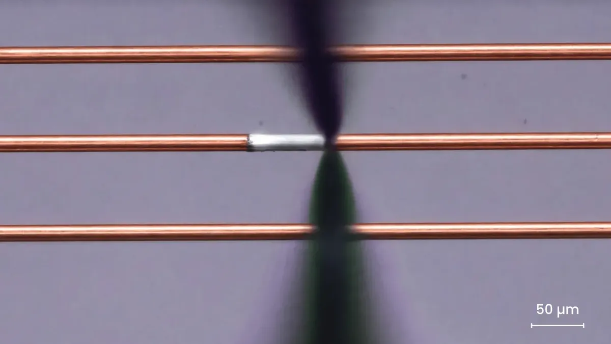
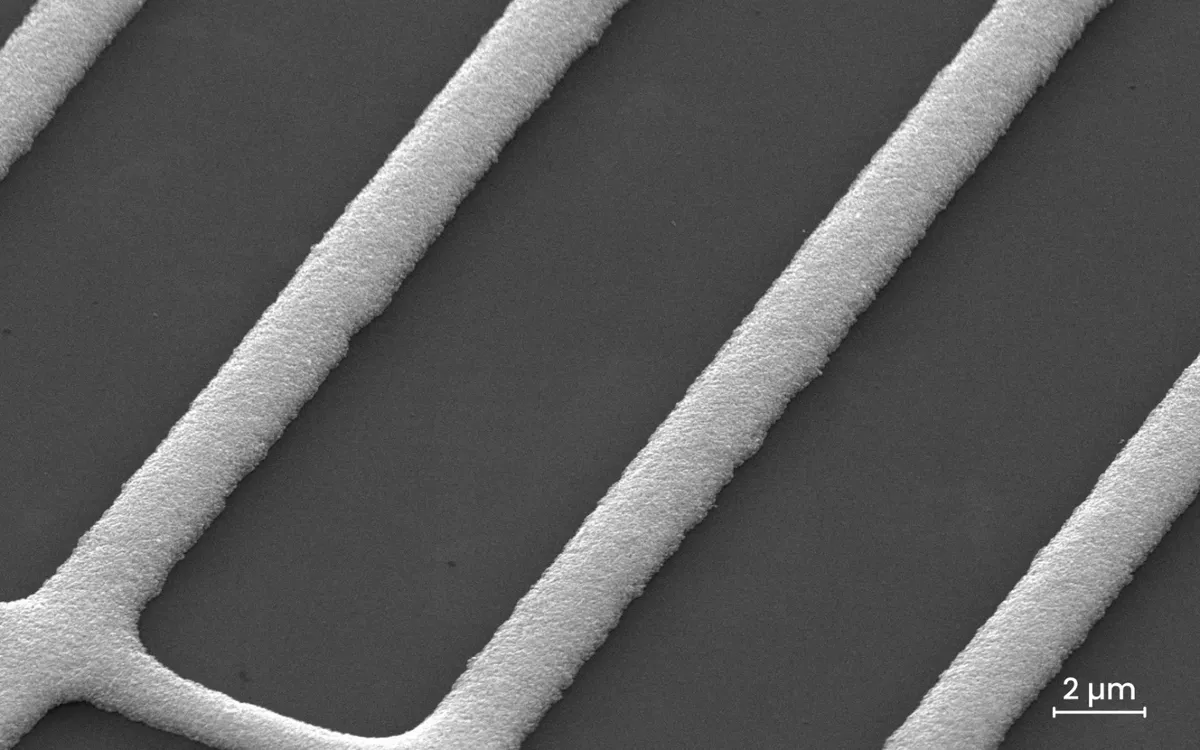
Repair of conductive lines from 50 μm down to 2 μm
HPCaP repairs conductive lines across this range, including the sub-15 μm range where no other solution exists.
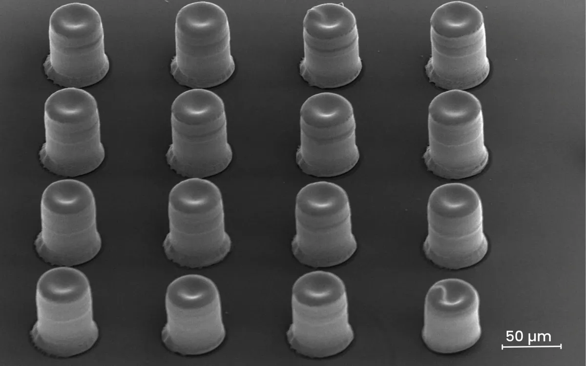
Repair of indium bumps from 5 to 50 μm
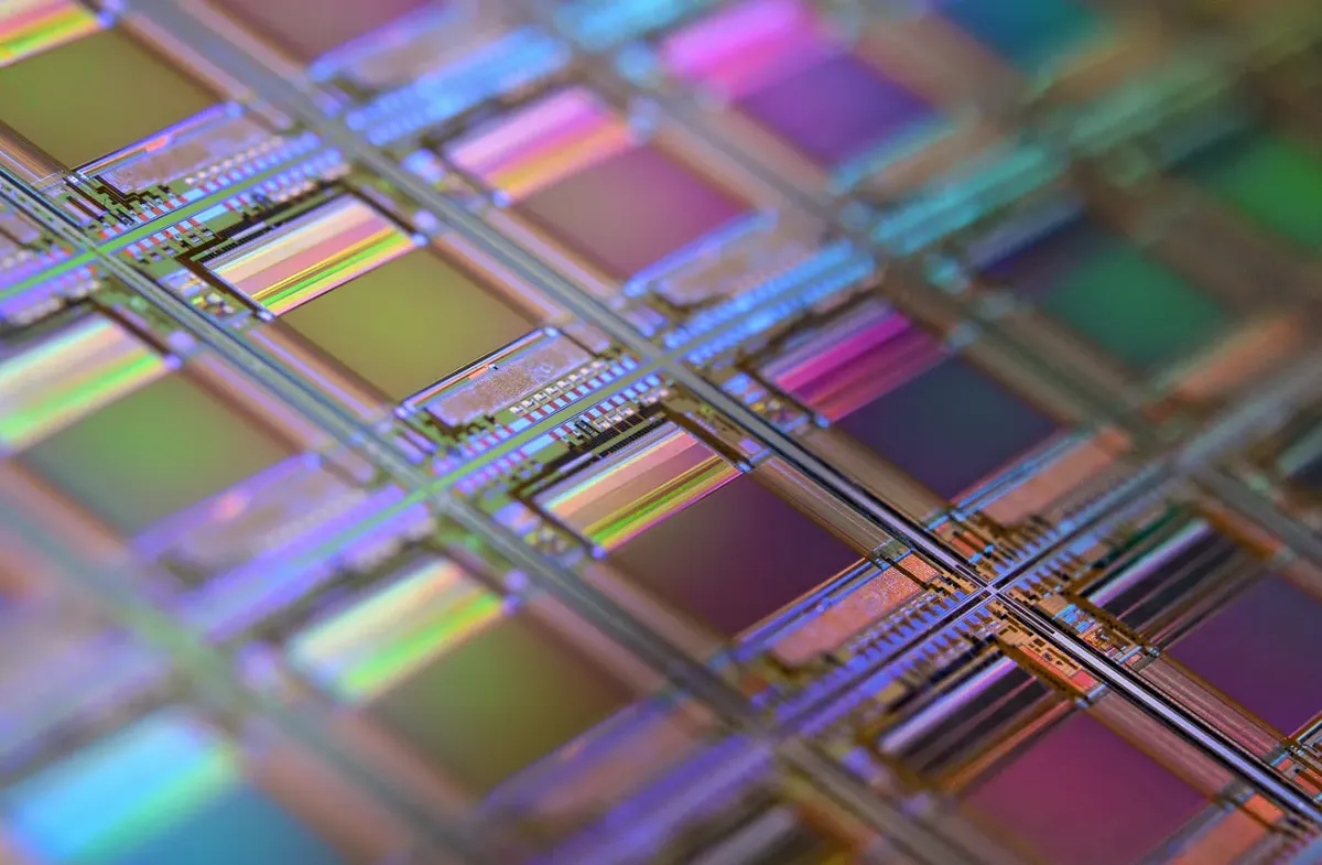
BIRD repairs bumps from 5 to 50 μm, with a focus on indium bumps. Indium is widely used for interconnects in demanding applications, and reliable bump repair helps recover assemblies that would otherwise be lost.
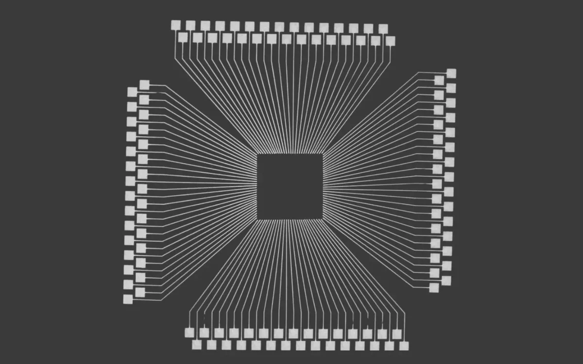
Deposits on display substrates
Examples of deposits made with HPCaP on display-relevant substrates.
Get started
Still unsure? We will help you find the right fit.
We’ll help you match the right inks and pipettes to your printing needs.