Field of application
Display & Display Repair
HPCaP enables targeted deposition of inks on display substrates, for production and defect repair
Market challenges
A resolution gap for open defect repair
TFT structures are now smaller than 5 μm, while the smallest open defects that existing technologies can repair measure 5 μm. Repair capability no longer matches panel resolution.
No industrial solution is available yet
Display manufacturers need repair that combines precision, throughput, and repeatability at production scale. No available solution meets all three today.
Particle contamination defects remain out of reach
Defects caused by particle contamination during manufacturing cannot currently be repaired. Addressing them would widen the range of recoverable panels.
Scrap and redundancy as the default response
Defective panels are discarded or compensated with redundancy, meaning spare components and backup circuits. Redundancy takes up panel space and limits layout optimization.

How HPCaP addresses them
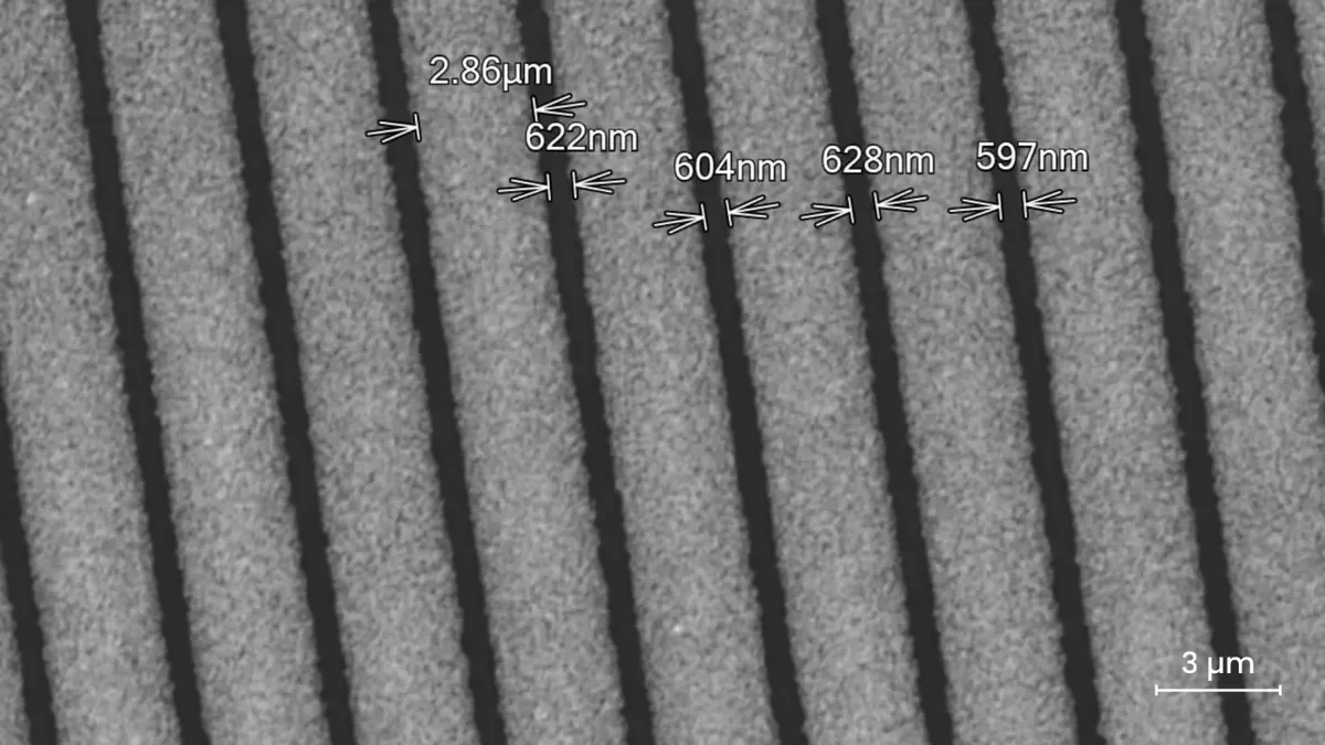
Resolution matched to TFT structures
HPCaP is qualified down to 2 μm, below the 5 μm limit of existing repair technologies. Open defects can be repaired at the scale of current TFT structures.
Functional metal deposition on any substrate
HPCaP deposits metal with an electrical conductivity of up to 30% of the bulk material. Automatic calibration follows the topography of the substrate, so the process adapts to different surfaces and conductivities.
Open defect repair and cavity filling in one tool
The same technology repairs open defects and fills cavities, including in the planarization layer.
Repair at several manufacturing steps
HPCaP can be applied at multiple stages of display fabrication, for OLED, microLED, and LCD. Repairing the defect directly frees the space used by redundancy and helps preserve display performance.
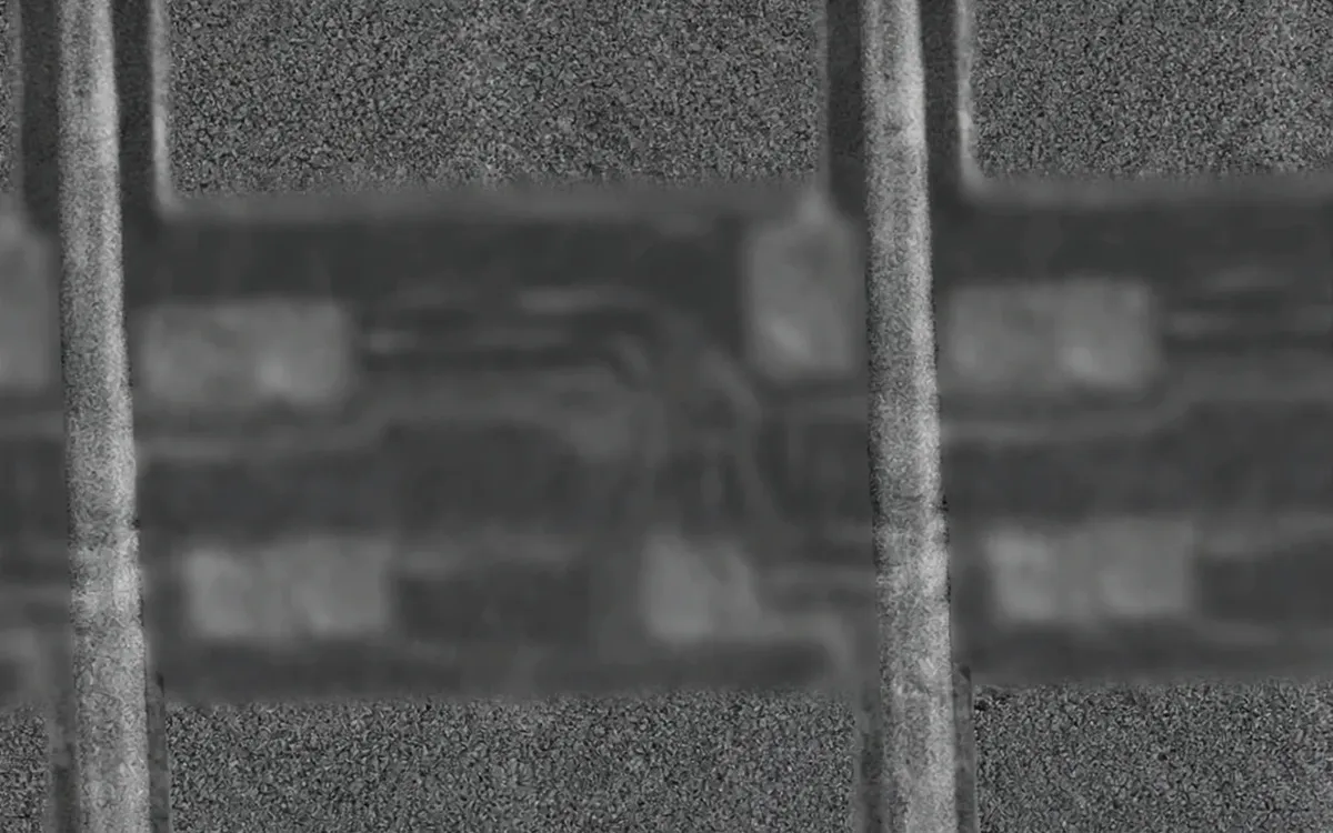
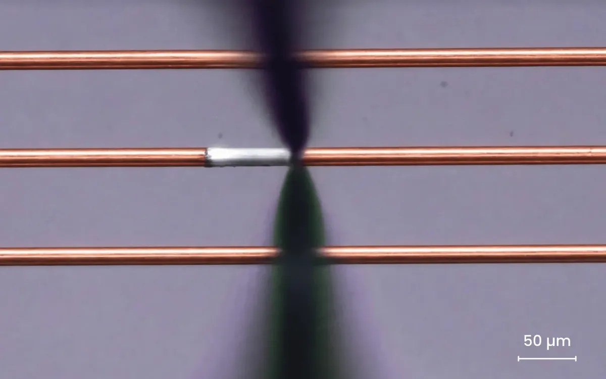
Deposits on display substrates
Examples of deposits made with HPCaP on display-relevant substrates.
Get started
Still unsure? We will help you find the right fit.
We’ll help you match the right inks and pipettes to your printing needs.